Nmos Transistor Circuit Diagram
Transistor nmos source Nmos transistor layout with a deep n-well Pmos nmos transistors
MOSFET | Electronics Tutorial
23 layout diagram of the hv nmos transistor. Energy band diagrams of pmos and nmos transistors under inversion bias I 0 v characteristics of a hv nmos transistor as a function of
Difference between nmos, pmos, cmos transistor with symbols
Solved the nmos transistors in the circuit of the followingNmos pmos transistors Nmos transistor mosfet semiconductorNmos transistor mosfet cmos structure drain terminal gate body physical source current diode oxide transistors terminals basic silicon junction channel.
Nmos transistor in layoutNmos circuit diagram Transistor nmos hv temperature1. schematic cross section and symbol of an nmos transistor. all the.

Circuit diagram of nor gate using cmos
Mosfet transistors mos terminal body schematic electronics tutorial electronic devicesNmos pmos transistor Consider the following nmos inverter circuit which consists of twoNmos layout transistor hv.
Nmos transistor vtoNmos transistor layout The symbol of (a) a pmos transistor and (b) an nmos transistorReverse-engineering the z-80: the silicon for two interesting gates.

Pmos circuit diagram
Nmos circuit solved transcribed problem text been show hasNmos transistor : cross section, working, circuit & its differences Solved 1) the nmos transistor in the circuit below has theLayout of cmos circuits nmos transistor symbolic layout (stick diagram ).
Layout cmos nmos transistor diagram stick symbolic circuits analog integrated circuit studylib8: circuit diagram of nmos test transistor. Transistor silicon nmos diffusion transistors oxide cpu hackaday rightoNmos transistor.

How a mosfet works at the semiconductor level -…
Simple nmos transistor circuit output impedance2. the nmos transistor in the discrete cs amplifier circuit of fig. 2 Nmos connection diode transistorNmos transistor cmos conductor schematic logic bad why good but high circuit low circuitlab created using stack.
Data sit trasistorTransistor diode nmos structure cmos does two diagram transistors interconnecting relate its stack electronics Nmos transistor in diode connection.Nmos transistor symbol.
Nmos transistor amplifier discrete biased 4ma homeworklib jp2 jl jpi fp3
Cmos pmos nmos sit transistors transistor data difference between trasistorSchematic cross section of a nmos transistor. (a) the transistor shown Download scientific diagramNmos inverter consists consider enhancement calculate nml transistors.
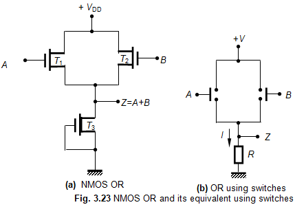
Draw a 3-d physical structure of an nmos transistor. label fourSolved the nmos and pmos transistors in the below circuit Nmos or gate circuit ~ electronics and communicationNmos and pmos transistors structure.

Nmos gate circuit table
Nmos transistors and pmos transistors explainedNmos circuit transistor output impedance simple transistors ignored equal effect both body stack Pmos nmos transistor cmos transistors operation voltageCircuit pmos nmos understanding stack containing pmosfet nmosfet happening troubles exactly having.
.


physics - CMOS: Why is an nMOS transistor a bad conductor of high logic

Difference between NMOS, PMOS, CMOS Transistor with Symbols - ETechnoG

1. Schematic cross section and symbol of an NMOS transistor. All the

How a MOSFET works at the Semiconductor level -… | CircuitBread

MOSFET | Electronics Tutorial

NMOS Transistors and PMOS Transistors Explained | Built In